(China (Mainland))

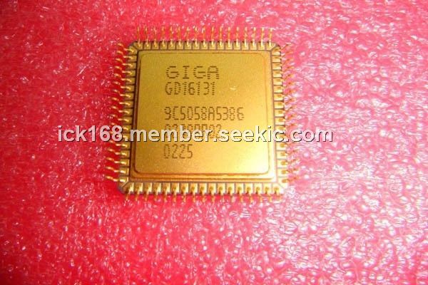
Product Summary
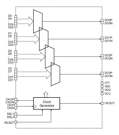
The GD16131 is a 622 Mbit/s MUX/DeMUX Chip Set. It is made as four identical blocks of 8 bit and a clock driver circuit. The 8 bit blocks are implemented as shift registers to obtain the best speed/power ratio of the process technology used. The GD16131 is packaged in 68 pin Multi Layer Ceramic(MLC) packages, yielding excellent highspeed signal accommodation and thermal conditions.
Parametrics
GD16131 absolute maximum ratings: (1)VEE Negative Supply: min=-7 V, max=0 V; (2)VCC Positive Supply: min=0, max=+7 V; (3)VO max ECL Output Voltage: min=VEE -0.5 V, max=0.5 V; (4)VO max TTL Output Voltage: min=-0.5 V, max=VCC +0.5 V; (5)IO max ECL Output Current: max=40 mA; (6)IO max TTL Output Current: max=20 mA; (7)VI max ECL Input Voltage: min=VEE -0.5 V, max=0.5 V; (8)VI max TTL Input Voltage: min=-0.5 V, max=VCC +0.5 V; (9)II max ECL Input Current: min=-1.0 mA, max=1.0 mA; (10)II max TTL Input Current: min=-1.0 mA, max=1.0 mA.
Features
GD16131 features: (1)Quad 8:1 MUX; (2)All high-speed I/O are differential, ECL level; (3)All low-speed I/O are TTL level, outputs drive 10 pF at 78 MHz; (4)Subdivided output clock to data relation selectable in four phases; (5)Dual supply: +5 V, -5.2 V; (6)68 pin MLC flat package; (7)High-speed pins on single side of package for easy PCB routing; (8)Power consumption: 1.3 W typical.
Diagrams
 |
 GD16521 |
Other |
|
Data Sheet |
Negotiable |
|
||||
|
GD16578 |
Other |
|
Data Sheet |
Negotiable |
|
||||